How ChipForge Validates Chip Designs
Every hardware design problem on ChipForge starts with two questions before it is launched as a challenge for miners.
Is this problem worth solving?
And just as important: can we validate the solutions properly?
The first question is usually the easy one.
If a design problem is useful for the community, useful for the industry, and useful for the future of open hardware, then it is worth turning into a challenge.
The second question is where the real work begins.
The Challenge Behind Every Hardware Design
Because in our subnet, launching a challenge does not just mean publishing a task and waiting for submissions. It means building a validation pipeline strong enough to judge real hardware work. On Bittensor, subnets are incentive systems, and the validator's job is to decide what actually creates value. In our case, that value is not text, rankings, or API responses. It is chip design.
So before a challenge goes live, we have to know that the pipeline can answer the questions that matter.
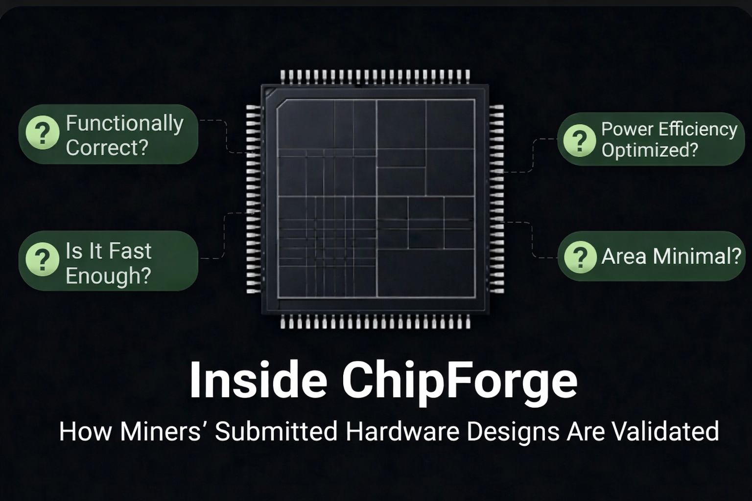
Is the design functionally correct? How much area does it take? How much power does it use? How fast is it? Does it meet performance requirements? And above all: have we tested it enough?

That last question is the hardest one in all of chip design.
"Have We Tested It Enough?" — The Question That Consumes 70% of Every Chip
In semiconductor engineering, functional verification is widely described as the main bottleneck, and it is often cited as consuming more than 70% of the total design effort as chip complexity rises.
That is the part outsiders often miss.
People sometimes assume launching a hardware challenge should be quick, and that the time should mainly be spent by miners solving it. In software, that assumption can make sense. In hardware, it does not. A challenge is only real if the validation behind it is real. If we cannot measure it correctly, score it correctly, and stress it correctly, then we have not launched a serious challenge — we have only launched noise.
This is where functional coverage comes in.
When we verify hardware, we do not assume the design is clean. We assume there are bugs in it, because there always are. Some are obvious. Some take months to expose. The job of the validation pipeline is to keep pushing the design into scenarios where those bugs show up.
That sounds simple until you look at the math.
You Cannot Brute-Force Hardware
Take a plain 64-bit adder. It has two 64-bit inputs, which means 2¹²⁸ possible input combinations, about 3.4 × 10³⁸ cases.
Now imagine trying to test all of them.
Even under an extremely optimistic assumption, where a high-end GPU like the NVIDIA GeForce RTX 5090 could test tens of trillions of cases per second with perfect efficiency, it would still take on the order of 10¹⁷ years to exhaustively verify every combination.
That is longer than the age of the universe by many orders of magnitude.
So “fully tested” and “tested enough” are not the same thing.
And this is just an adder.
In real processor verification, the problem grows far beyond this. Verification must cover instruction sequences, corner cases, state interactions, and long execution flows across the entire system. Research literature consistently shows that the number of possible states and interactions grows too quickly to test exhaustively, especially once designs move beyond simple blocks into full cores and systems.
Hardware teams rely on simulation, constrained-random testing, coverage-driven verification, fuzzing, and formal methods together, not because they are optional, but because brute force does not scale.
You are not trying to test everything.
You are trying to break the design, as early as possible.

Every Improvement is a New Verification Challenge
Now take one step up from an adder and look at a processor.
A processor is not just adding numbers. It has pipelines, hazards, stalls, memory interactions, exceptions, control-flow changes, long instruction sequences, and many pieces of state moving at once. A recent survey of RISC-V processor verification notes that processor verification is complex precisely because it must cover instructions, software-hardware interaction, and many processor states, and it cites pre-release commercial testing on the order of 10¹⁶ test cycles for ARM devices.
That is why even a "small" architectural change is not small.
If a miner improves one block in a processor or NPU, we do not get to say, "great, that one block looks better." We have to ask what that change did to the rest of the machine. Did it break a corner case? Did it change timing? Did it create a new interaction with memory? Did it alter behavior after thousands or millions of cycles? That is why regressions have to be rerun. And that is why, in our flow, validation does not really stop. Early pipeline runs may cover hundreds of millions of instructions just to filter the field, and the strongest designs then keep getting stressed further. In real chip work, verification continues until tapeout, because confidence is built gradually, not declared once. Rising complexity and falling first-time-silicon success across the industry are exactly why design and verification have both become more time-consuming.
The Exponential Price of a Late Discovery
A software bug is painful, but usually recoverable. A patch goes out, systems update, and the issue is fixed. A silicon bug is different because the cost depends on when it is found. If it is caught during the frontend phase — while the team is still writing RTL — the fix is straightforward: update the HDL, re-simulate, and move on. But if the design has already moved into the backend, where RTL has been synthesized down to gates and transistors, placed on a floorplan, and routed — then a bug means going back to the frontend, fixing it there, and running the entire verification cycle again. Even when the testcases already exist, that re-verification alone can take months. If the bug escapes further and is found after fabrication, the consequences are far worse: another mask set, another manufacturing cycle, and sometimes replacement in the field. One of the best-known examples is Intel's Pentium FDIV bug, which reportedly cost the company about $475 million.

We Broke Google's NPU and then we Fixed it
As our team moves into NPU design, we chose Google's Coral NPU, an open-source RISC-V-based AI accelerator, as our baseline rather than building from scratch. Starting in November 2025, we began building our verification environment for this design: a custom test case generator paired with open-source simulation tools to run those tests against the NPU at scale. By mid-December, that infrastructure found a functional bug in the Coral NPU. We reported it, contributed the fix, and it was merged. Since then, we have found two more bugs that are currently in the fixing stage.
This is a good example of why verification takes time. Even with experienced teams and well-structured processes, bugs can still escape if the design has not been tested enough. For a design like the Coral NPU, thorough verification realistically requires six months or more of building test infrastructure, generating coverage, and running stress tests at scale. Our verification environment caught these issues because it was built with that level of rigor, and it is exactly the kind of industrial-grade infrastructure that every ChipForge challenge is built on.
Not Fast. Correct.
So when someone asks why ChipForge takes time to launch a challenge, the answer is simple:
Because a hardware challenge is not ready when the idea is ready.
It is ready when the validation pipeline is ready.
That is the standard.
And that standard is exactly why this subnet matters.
Want to contribute?
Join our network of engineers building the future of chip design.